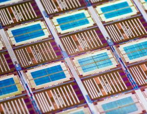
Green Mountain Semiconductor Awarded a NASA Phase II Contract for Innovative Compute-In-Memory Architecture
Non-volatile memory for weight storage on-chip reduces data movements and allows for low power, low latency edge AI inferencing in high radiation environments.
BURLINGTON, VERMONT, USA, May 1, 2024 /EINPresswire.com/ -- Green Mountain Semiconductor Inc, a leading design house specializing in AI-related circuit design initiatives since 2014, has secured a Phase II contract from NASA. This achievement follows the successful completion of Phase I and underscores Green Mountain Semiconductor's commitment to advancing cutting-edge technology for space exploration.The Compute-In-Memory architecture developed by Green Mountain Semiconductor, with sponsorship from NASA, represents a significant breakthrough in edge AI inferencing for radiation-laden environments. This architecture integrates non-volatile memory directly on-chip, reducing data movements and enabling low-power, low-latency AI inferencing.
Green Mountain Semiconductor's expertise in AI-related circuit design, coupled with its focus on Custom Analog, Digital, and Mixed Signal Design with a focus on Memory (DRAM, SRAM, and Emerging NVM), has positioned the company as a front runner in this field. The development of ultra-low power processing in-memory neural networks has been a key focus area, leading to groundbreaking innovations.
The foundation of the robust Compute-In-Memory architecture dates back to 2016 and has resulted in the filing of seven core patents. By incorporating a radiation-hardened Non-Volatile RAM for low power and low latency edge AI devices, this architecture eliminates the Von Neumann bottleneck, integrating all memory for weight storage on the chip, significantly reducing weight movement and decreasing the total amount of SRAM, as well as the length of time data is stored in SRAM. Focusing on SRAM reduction coupled with circuit design techniques, using radiation-hard NVM and radiation-hardened logic, the chip will reach radiation target levels required for deep space computing. This design optimization allows for accelerated AI inferencing, outperforming other state-of-the-art architectures.
"We are excited to advance our partnership with NASA on this innovative architecture and to be able to prove it into silicon," said Wolfgang Hokenmaier, President at Green Mountain Semiconductor. "Our concept represents a departure from existing methodologies; it addresses both the highest performance expectations for on-board edge AI processing and the radiation-hard environments constraints in a single solution."
The potential applications of this architecture include NASA space missions with critical image processing where device functionality is imperative, as well as autonomous vehicles and systems operating in isolated and harsh environments with safety-critical constraints.
About Green Mountain Semiconductor
Green Mountain Semiconductor is a design services, consulting, and intellectual property company headquartered in Burlington, Vermont. The company's research and development efforts are centered on memory chips capable of handling key repetitive tasks traditionally managed by CPUs. This approach reduces overall data transport needs and eliminates the 'memory bottleneck' that often hinders computing performance, which has implications for high complexity neuromorphic computing applications and low power devices including medical and IoT devices. Green Mountain Semiconductor offers a comprehensive range of services to its clients, including circuit design, characterization, and testing. Learn more at www.greenmountainsemi.com.
For media inquiries, please contact:
WOLFGANG HOKENMAIER
Green Mountain Semiconductor
+1 802-343-8175
email us here
Visit us on social media:
LinkedIn
EIN Presswire does not exercise editorial control over third-party content provided, uploaded, published, or distributed by users of EIN Presswire. We are a distributor, not a publisher, of 3rd party content. Such content may contain the views, opinions, statements, offers, and other material of the respective users, suppliers, participants, or authors.


